- 您现在的位置:买卖IC网 > Sheet目录1227 > MAX16929EVKIT+ (Maxim Integrated Products)KIT EVALUATION FOR MAX16929
�� �
�
�MAX16929�
�Automotive� TFT-LCD� Power� Supply� with� Boost�
�Converter� and� Gate� Voltage� Regulators�
�1.8V/3.3V� Regulator� Controller�
�The� 1.8V/3.3V� regulator� controller� delivers� 4.5mA� (min)�
�to� an� external� load.� Connect� FB� to� DR� for� a� regulated�
�1.8V/3.3V� output.�
�For� higher� output� capability,� use� an� external� npn� transis-�
�tor� as� shown� in� the� Typical Application Circuit� .� The� drive�
�capability� of� the� regulator� is� then� increased� by� the� cur-�
�rent� gain� of� the� transistor� (h� FE� ).� When� using� an� external�
�transistor,� use� DR� as� the� base� drive� and� connect� FB� to�
�the� transistor’s� emitter.� Bypass� the� base� to� ground� with� a�
�0.1� F� F� ceramic� capacitor.�
�If� the� boost� output� current� is� greater� than� 300mA,� con-�
�nect� a� 30k� I� resistor� between� DR� and� GND.�
�Positive-Gate� Voltage� Regulator� (GH)�
�The� positive-gate� voltage� regulator� includes� a� p-channel�
�FET� output� stage� to� generate� a� regulated� output� between�
�+5V� and� V� CP� -� 2V.� The� regulator� maintains� accuracy� over�
�wide� line� and� load� conditions.� It� is� capable� of� at� least�
�20mA� of� output� current� and� includes� current-limit� protec-�
�tion.� V� GH� is� typically� used� to� provide� the� TFT-LCD� gate�
�drivers’� gate-on� voltage.�
�The� regulator� derives� its� positive� supply� voltage� from� a�
�noninverting� charge� pump,� a� single-stage� example� of�
�which� is� shown� in� the� Typical Application Circuit� .� A� high-�
�er� voltage� using� a� multistage� charge� pump� is� possible,�
�as� described� in� the� Charge Pumps� section.�
�Negative-Gate� Voltage� Regulator� (GL)�
�The� negative-gate� voltage� regulator� is� an� analog� gain�
�block� with� an� open-drain� p-channel� output.� It� drives� an�
�external� npn� pass� transistor� with� a� 6.8k� I� base-to-emitter�
�resistor� (see� the� Pass Transistor Selection� section).� Its�
�guaranteed� base� drive� source� current� is� at� least� 2mA.�
�V� GL� is� typically� used� to� provide� the� TFT-LCD� gate� driv-�
�ers’� gate-off� voltage.�
�The� output� of� the� negative-gate� voltage� regulator� (i.e.,�
�the� collector� of� the� external� npn� pass� transistor)� has� load-�
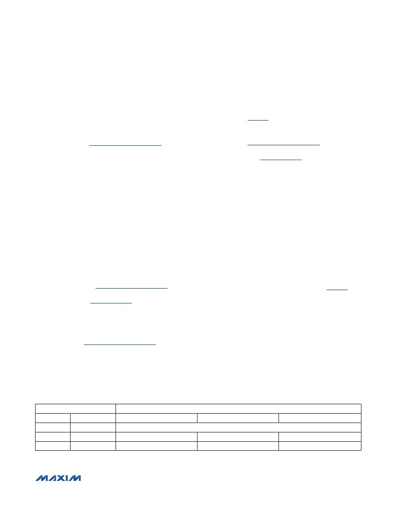
�Table 1. Supply Sequencing�
�CONTROL INPUTS�
�dependent� bypassing� requirements.� Connect� a� ceramic�
�capacitor� between� the� collector� and� ground� with� the�
��The� regulator� derives� its� negative� supply� voltage� from� an�
�inverting� charge� pump,� a� single-stage� example� of� which�
�is� shown� in� the� Typical Application Circuit� .� A� more� nega-�
�tive� voltage� using� a� multistage� charge� pump� is� possible�
�as� described� in� the� Charge Pumps� section� .�
�The� external� npn� transistor� is� not� short-circuit� protected.�
�To� maintain� proper� pulldown� capability� of� external� npn�
�transistor� and� optimal� regulation,� a� minimum� load� of� at�
�least� 500μA� is� recommended� on� the� output� of� the� GL�
�regulator.�
�Enable� (ENP)�
�Use� the� enable� input� (ENP)� to� enable� and� disable� the�
�boost� section� of� the� device.� Connect� ENP� to� INA� for�
�normal� operation� and� to� GND� to� place� the� device� in� shut-�
�down.� In� shutdown,� the� INA� supply� current� is� reduced� to�
�0.5� F� A.�
�Soft-Start� and� Supply� Sequencing� (SEQ)�
�When� enabled,� the� boost� output� ramps� up� from� V� INA� to�
�its� set� voltage.� Once� the� boost� output� reaches� 85%� of� the�
�set� voltage� and� the� soft-start� timer� expires,� the� gate� volt-�
�age� regulators� turn� on� in� the� order� shown� in� Table 1� .� The�
�1.8V/3.3V� regulator� controller� is� enabled� at� the� beginning�
�of� the� boost� converter’s� soft-start.�
�Both� gate� voltage� regulators� have� a� 7.45ms� soft-start�
�time.� The� second� one� turns� on� as� soon� as� the� output� of�
�the� first� reaches� 85%� of� its� set� voltage.�
�Thermal� Shutdown�
�Internal� thermal� shutdown� circuitry� shuts� down� the�
�device� immediately� when� the� die� temperature� exceeds�
�+165� N� C.� A� 15� N� C� thermal� shutdown� hysteresis� prevents�
�the� device� from� resuming� normal� operation� until� the� die�
�temperature� falls� below� +150� N� C.�
�SUPPLY SEQUENCING�
�ENP�
�0�
�1�
�1�
�SEQ�
�X�
�0�
�1�
�FIRST�
�V� SH�
�V� SH�
�SECOND�
�Device� is� in� shutdown�
�V� GH�
�V� GL�
�THIRD�
�V� GL�
�V� GH�
� ????????????????????????????????????????????????????????????????� � Maxim� Integrated� Products� � � 15�
�发布紧急采购,3分钟左右您将得到回复。
相关PDF资料
MAX16946EVKIT+
KIT EVALUATION FOR MAX16946
MAX17015EVKIT+
KIT EVAL FOR MAX17015
MAX17021EVKIT+
EVAL KIT FOR MAX17021
MAX1702EVKIT
EVAL KIT FOR MAX1702
MAX17710EVKIT#
RD ENERGY HARVESTING
MAX19000EVKIT+
EVAL KIT MAX19000
MAX19710EVKIT+
EVAL KIT FOR MAX19710
MAX1978EVKIT
EVAL KIT MAX1978
相关代理商/技术参数
MAX16929FGUI/V+
功能描述:LCD 驱动器 18V 2MHz Auto TFT-LCD Pwr Supply RoHS:否 制造商:Maxim Integrated 数位数量:4.5 片段数量:30 最大时钟频率:19 KHz 工作电源电压:3 V to 3.6 V 最大工作温度:+ 85 C 最小工作温度:- 20 C 封装 / 箱体:PDIP-40 封装:Tube
MAX16929FGUI/V+T
功能描述:LCD 驱动器 18V 2MHz Auto TFT-LCD Pwr Supply RoHS:否 制造商:Maxim Integrated 数位数量:4.5 片段数量:30 最大时钟频率:19 KHz 工作电源电压:3 V to 3.6 V 最大工作温度:+ 85 C 最小工作温度:- 20 C 封装 / 箱体:PDIP-40 封装:Tube
MAX16929GGUI/V+
功能描述:LCD 驱动器 18V 2MHz Auto TFT-LCD Pwr Supply RoHS:否 制造商:Maxim Integrated 数位数量:4.5 片段数量:30 最大时钟频率:19 KHz 工作电源电压:3 V to 3.6 V 最大工作温度:+ 85 C 最小工作温度:- 20 C 封装 / 箱体:PDIP-40 封装:Tube
MAX16929GGUI/V+T
功能描述:LCD 驱动器 18V 2MHz Auto TFT-LCD Pwr Supply RoHS:否 制造商:Maxim Integrated 数位数量:4.5 片段数量:30 最大时钟频率:19 KHz 工作电源电压:3 V to 3.6 V 最大工作温度:+ 85 C 最小工作温度:- 20 C 封装 / 箱体:PDIP-40 封装:Tube
MAX16929GUI/V+
功能描述:LCD 驱动器 18V 2MHz Auto TFT-LCD Pwr Supply RoHS:否 制造商:Maxim Integrated 数位数量:4.5 片段数量:30 最大时钟频率:19 KHz 工作电源电压:3 V to 3.6 V 最大工作温度:+ 85 C 最小工作温度:- 20 C 封装 / 箱体:PDIP-40 封装:Tube
MAX16929GUI/V+T
功能描述:LCD 驱动器 18V 2MHz Auto TFT-LCD Pwr Supply RoHS:否 制造商:Maxim Integrated 数位数量:4.5 片段数量:30 最大时钟频率:19 KHz 工作电源电压:3 V to 3.6 V 最大工作温度:+ 85 C 最小工作温度:- 20 C 封装 / 箱体:PDIP-40 封装:Tube
MAX16929HGUI/V+
功能描述:LCD 驱动器 18V 2MHz Auto TFT-LCD Pwr Supply RoHS:否 制造商:Maxim Integrated 数位数量:4.5 片段数量:30 最大时钟频率:19 KHz 工作电源电压:3 V to 3.6 V 最大工作温度:+ 85 C 最小工作温度:- 20 C 封装 / 箱体:PDIP-40 封装:Tube
MAX16929HGUI/V+T
功能描述:LCD 驱动器 18V 2MHz Auto TFT-LCD Pwr Supply RoHS:否 制造商:Maxim Integrated 数位数量:4.5 片段数量:30 最大时钟频率:19 KHz 工作电源电压:3 V to 3.6 V 最大工作温度:+ 85 C 最小工作温度:- 20 C 封装 / 箱体:PDIP-40 封装:Tube